Product Summary
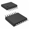
The SN74LV06APWR is a HEX inverter buffer/driver with open-drain outputs. The SN74LV06APWR is fully specified for partial-power-down applications using Ioff.
Parametrics
SN74LV06APWR absolute maximum ratings: (1)Supply voltage range, VCC: 0.5 V to 7 V; (2)Input voltage range, VI: 0.5 V to 7 V; (3)Voltage range applied to any output in the high-impedance or power-off state, VO: 0.5 V to 7 V; (4)Input clamp current, IIK (VI < 0): 20 mA; (5)Output clamp current, IOK (VO < 0): 50 mA; (6)Continuous output current, IO (VO = 0 to VCC): 35 mA; (7)Continuous current through VCC or GND: ±50 mA; (8)Package thermal impedance, θJA D package: 86℃/W; (9)Package thermal impedance, θJA DB package: 96℃/W; (10)Package thermal impedance, θJA DGV package: 127℃/W; (11)Package thermal impedance, θJA NS package: 76℃/W; (12)Package thermal impedance, θJA PW package: 113℃/W; (13)Storage temperature range, Tstg: 65℃ to 150℃.
Features
SN74LV06APWR features: (1)2-V to 5.5-V VCC Operation; (2)Max tpd of 6.5 ns at 5 V; (3)Typical VOLP (Output Ground Bounce) <0.8 V at VCC = 3.3 V, TA = 25℃; (4)Typical VOHV (Output VOH Undershoot) >2.3 V at VCC = 3.3 V, TA = 25℃; (5)Outputs Are Disabled During Power Up and Power Down With Inputs Tied to GND; (6)Support Mixed-Mode Voltage Operation on All Ports; (7)Latch-Up Performance Exceeds 100 mA Per JESD 78, Class II.
Diagrams
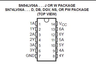
| Image | Part No | Mfg | Description |  |
Pricing (USD) |
Quantity | ||||||||||||
|---|---|---|---|---|---|---|---|---|---|---|---|---|---|---|---|---|---|---|
 |
 SN74LV06APWR |
 Texas Instruments |
 Buffers & Line Drivers Hex Inv w/HV Output |
 Data Sheet |

|
|
||||||||||||
 |
 SN74LV06APWRE4 |
 Texas Instruments |
 Buffers & Line Drivers Hex Inverter Driver |
 Data Sheet |

|
|
||||||||||||
 |
 SN74LV06APWRG4 |
 Texas Instruments |
 Buffers & Line Drivers Hex Inverter Buffers Drivers |
 Data Sheet |

|
|
||||||||||||
 (China (Mainland))


